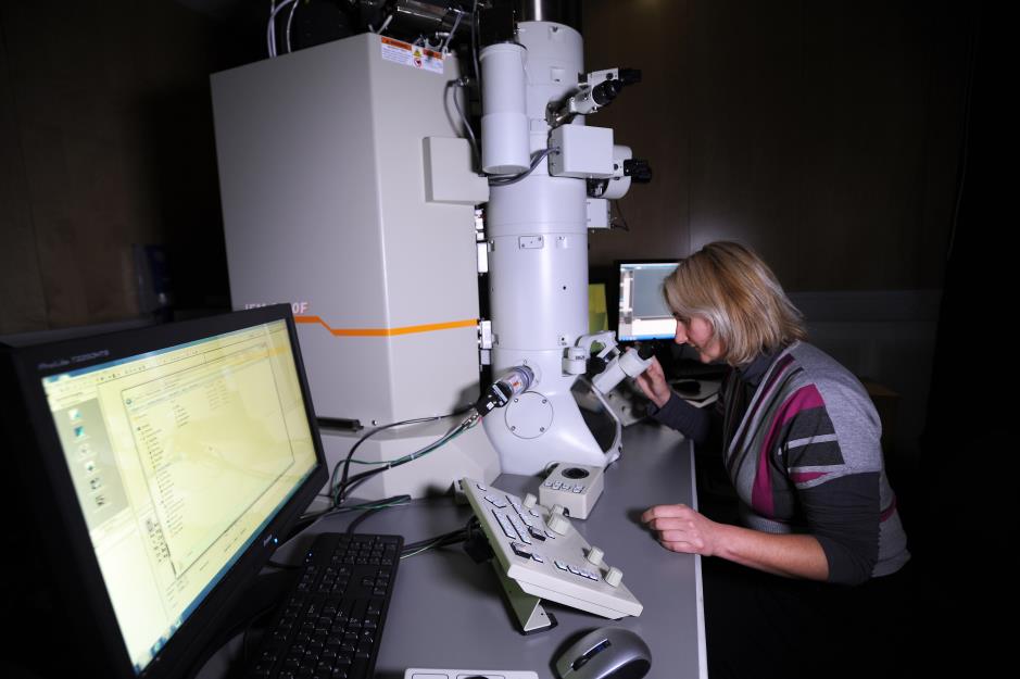
TEM cathodoluminescence and electron energy loss spectroscopy
Cathodoluminescence (CL) and Electron Energy Loss Spectroscopy (EELS) within our advanced TEM facilities provide powerful, complementary nanoscale characterisation capabilities for industry.
These techniques are highly relevant to a number of industries. CL offers spatially resolved insight into optical and electronic behaviour, while EELS delivers quantitative elemental, chemical and electronic structure information at the atomic scale. Together, they enable industry users to accelerate materials development, diagnose failure mechanisms, optimise processing routes and improve device performance.
CL and EELS is an extremely versatile technqiue that has applications that span across numerous sectors:
Semiconductors & Microelectronics
Our CL–EELS TEM facilities provide semiconductor and microelectronics companies with unrivalled insight into defects, interfaces and electronic structure at the nanoscale. We support rapid identification of yield‑limiting defects, dopant distribution, strain and band‑gap variations in materials such as GaN, SiC, silicon and emerging wide‑bandgap semiconductors. By linking structural, chemical and optoelectronic information in a single analysis, we help partners accelerate process development, improve device reliability and reduce costly trial‑and‑error during manufacturing scale‑up.
Energy Technologies (PV, Nuclear, Radiation‑Hard Materials)
For energy and sustainability sectors, our CL–EELS TEM capabilities enable detailed understanding of how defects, chemistry and microstructure impact performance and lifetime. We work with companies developing photovoltaic materials, battery components, scintillators and radiation‑hard materials to identify non‑radiative recombination pathways, degradation mechanisms and processing‑induced variability. The resulting insights help partners optimise materials design, extend operational lifetimes and de‑risk next‑generation energy technologies.
Photonics, Optoelectronics & Luminescent Materials
Our facilities are ideally suited to companies working in photonics, optoelectronics and luminescent materials, including emitters, phosphors, nanophotonic structures and quantum materials. Cathodoluminescence reveals where and why light emission is gained or lost at the nanoscale, while EELS provides complementary chemical and electronic structure information. Together, these techniques enable rapid optimisation of optical performance, support failure analysis and help shorten the path from materials discovery to deployable devices.
Advanced Coatings & Functional Nanomaterials
Our CL–EELS TEM facilities support companies developing advanced coatings and functional nanomaterials by revealing how nanoscale structure, composition and defects influence real‑world performance. We help partners optimise luminescent, protective and functional coatings, ceramics and powders by identifying inhomogeneities, processing‑induced defects and performance‑limiting interfaces. This detailed insight enables more reliable scale‑up, improved quality control and faster routes from materials development to robust commercial products.
Aerospace & Defence
For aerospace and defence applications, our CL–EELS TEM capabilities provide critical insight into materials performance under extreme conditions. We work with partners developing radiation‑hard, high‑reliability and space‑qualified materials to understand defect formation, degradation pathways and microstructural stability at the nanoscale. By linking chemical, structural and electronic or optical behaviour, we help companies de‑risk materials choices, improve component reliability and meet stringent qualification requirements.
Mining, Geology & High‑Value Materials
Our CL–EELS TEM facilities offer powerful tools for companies working with minerals, ores and high‑value natural materials. Cathodoluminescence enables rapid identification of growth zoning, defects and provenance signatures, while EELS provides complementary chemical and electronic structure information at high spatial resolution. Together, these techniques support mineral characterization, process optimisation, provenance studies and authentication of high‑value materials, delivering actionable insights that enhance exploration efficiency and materials valuation.
For more information or to discuss your TEM CL-EELS testing requirements, please contact Dr Wayne Lam at wayne.lam@brunel.ac.uk
You can return to our main Commercial Services page to see what else we have that could support your requirements.